
Intel introduced its first 4-bit microprocessor, the 4004, in 1971, and followed up with an 8-bit one, the 8008, in 1972. However, these early microprocessors had limitations in their design and performance, preventing them from being widely used as general-purpose microprocessors.
A breakthrough came in 1974 with the launch of the 8080, Intel’s first general-purpose 8-bit microprocessor, marking a significant step forward in microprocessor development. This was further refined with the introduction of the 8085, which added more features and resulted in a fully functional microprocessor.
Despite these advancements, 8-bit microprocessors still faced challenges like slow speeds, limited memory addressing, and fewer general-purpose registers, prompting designers to strive for more powerful processors with advanced architectures, greater processing capabilities, and improved instruction sets. The 8086 emerged from these efforts.
In 1978, Intel unveiled the 8086, its first 16-bit microprocessor, in response to the growing demand for faster and more powerful computational resources. The 8086 boasted a significantly enhanced instruction set and architectural improvements, providing greater programming flexibility and speed compared to its 8-bit predecessors.
Peripheral chips originally designed for the 8085 could be used with the 8086 with minor adjustments, despite differences in memory addressing techniques and clock requirements. The overall organization of the 8086 system resembled that of a general 8-bit microprocessor.
This article explores the architectures of the 8086 and its variant, the 8088, in detail, including how supporting chips interface with them to create a basic system. It also provides comprehensive insights into the organization of both the 8086 and 8088, along with essential timing diagrams.
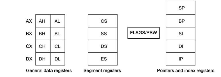
REGISTER ORGANIZATION OF 8086
The 8086 microprocessor has a powerful set of registers, which can be divided into two types: general-purpose registers and special-purpose registers.
- General Purpose Registers: These registers are versatile and can hold either 8 bits or 16 bits of data. They are used for storing data, variables, or temporary results. Additionally, they can function as counters or hold offset addresses for specific addressing modes.
- Special Purpose Registers: These registers serve specific functions such as segment registers, pointers, index registers, or storing offsets for particular addressing modes.
We can group the registers into four categories:
- General Purpose Registers (16-bit):
- These can hold 16 bits of data or be used as two 8-bit registers.
- Used for various purposes like data storage, variable handling, or as counters.
- Segment Registers:
- These are special-purpose registers used to store segment information for memory addressing.
- Pointer and Index Registers:
- These registers are special purpose and used for pointing to memory locations or indexing operations.
- Offset Storage Registers:
- Special purpose registers used to store offsets for specific addressing modes.
In summary, the 8086 registers provide flexibility for storing data, managing memory addressing, and performing arithmetic and logic operations.
General Data Registers
The general data registers in the 8086 microprocessor are versatile registers that can hold either 8 bits or 16 bits of data. They are used for various purposes such as storing data, variables, or temporary results. These registers can also function as counters or hold offset addresses for specific addressing modes. Here are the full details:
- Versatility: These registers are capable of holding either 8 bits (one byte) or 16 bits (two bytes) of data. This flexibility allows them to adapt to different data types and operations.
- Purpose: The primary function of these registers is to store data during program execution. They can hold variables, constants, or temporary results generated during arithmetic or logical operations.
- Usage as 16-bit or 8-bit Registers: Each of these general data registers can be accessed either as a whole 16-bit register or as two separate 8-bit registers. When used as 16-bit registers, they provide the capability to handle larger data sizes or memory addresses. When used as 8-bit registers, they allow for more efficient manipulation of smaller data sizes.
- Common Operations: These registers are frequently used for arithmetic operations, logical operations, data movement instructions (such as loading data from memory or storing data to memory), and addressing calculations.
- Examples: In the 8086 architecture, the general data registers include:
- AX: Accumulator Register
- BX: Base Register
- CX: Counter Register
- DX: Data Register
- Role in Programming: Programmers utilize these registers extensively in assembly language programming to perform computations, manipulate data, and control program flow.
- Temporary Storage: These registers are often used to hold intermediate results during calculations or data transformations. They provide fast access to data, which is crucial for efficient program execution.
Segment Registers
In simple terms, the 8086 microprocessor organizes memory differently from the 8085. Instead of one continuous block of memory, it divides memory into smaller chunks called segments. Each segment is like a folder containing 64 kilobytes (KB) of memory.
To keep track of these segments, the 8086 has four special registers:
- Code Segment Register (CS): Points to where the program’s instructions are stored.
- Data Segment Register (DS): Points to where the program’s data is stored.
- Extra Segment Register (ES): Another register that can be used to store additional data.
- Stack Segment Register (SS): Points to where the program’s stack is stored. The stack is used to temporarily hold important data.
When the processor wants to access a specific memory location, it combines the segment address from one of these registers with an offset address from another register. This combination forms the physical memory address where the data is stored.
The benefit of this system is that the processor only needs to keep track of two 16-bit registers instead of one 20-bit register, which makes things simpler and faster. These segment registers hold the starting addresses of different parts of memory, but they don’t necessarily represent physically separate memory areas. In other words, multiple segments could be stored in the same memory chip, or a single segment might span across multiple chips.
Pointers and Index Registers
Pointers and index registers in the 8086 microprocessor are special registers used for memory addressing and data manipulation. Here’s an easy-to-understand explanation:
- Pointers: Pointers are registers that hold memory addresses. They “point” to specific locations in memory where data is stored. Programmers use pointers to access and manipulate data indirectly, by referencing the memory addresses stored in these registers.
- Index Registers: Index registers are like counters that help with accessing data in arrays or tables. They hold a value that is used as an offset or index to access elements within a data structure. By incrementing or decrementing the value in the index register, programmers can navigate through arrays or other data structures efficiently.
Together, pointers and index registers provide powerful tools for managing memory and accessing data in the 8086 microprocessor. They enable programmers to work with complex data structures and perform operations on large sets of data more easily.
Flag Register
The Flag Register in the 8086 microprocessor is a special register that holds status flags indicating the outcome of arithmetic and logical operations. Here’s a straightforward explanation:
- Status Flags: The Flag Register contains several individual flags, each representing a specific condition or status of the processor after an operation.
- Common Flags:
- Zero Flag (ZF): Set if the result of an operation is zero.
- Sign Flag (SF): Set if the result of an operation is negative.
- Carry Flag (CF): Set if an arithmetic operation generates a carry or borrow out of the most significant bit.
- Overflow Flag (OF): Set if the result of a signed operation exceeds the maximum or minimum value representable in the given data size.
- Parity Flag (PF): Set if the number of set bits in the result is even.
- Auxiliary Carry Flag (AF): Used for binary-coded decimal (BCD) arithmetic operations.
- Usage: Programmers can check these flags to make decisions based on the outcome of previous operations. For example, they might use the Zero Flag to determine if a result is zero, or the Carry Flag to detect overflow in arithmetic operations.
- Conditional Branching: Instructions in assembly language often use these flags to perform conditional branching, where the program execution path depends on the state of certain flags.
- Manipulation: Instructions are also available to modify these flags directly, allowing programmers to control the flow of execution based on specific conditions.
ARCHITECTURE
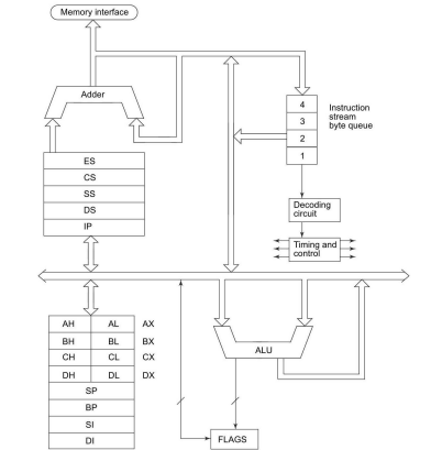
The 8086 architecture is an improvement over the 8085, with features like a 16-bit Arithmetic Logic Unit (ALU), 16-bit registers, segmented memory addressing, a wide instruction set, robust interrupt handling, and a queue for efficient instruction fetching and execution.
The architecture of the 8086 chip can be broken down into two main parts: the Bus Interface Unit (BIU) and the Execution Unit (EU).
- Bus Interface Unit (BIU): This unit handles physical address calculations and has a queue to store instruction bytes. It connects with external devices and memory through the system’s bus, facilitating communication with peripherals. The BIU plays a key role in managing data flow between the processor and external components.
- Execution Unit (EU): This unit executes instructions and performs computations. It works closely with the BIU to fetch instructions and process data. The EU is responsible for carrying out the operations specified by the instructions fetched from memory.

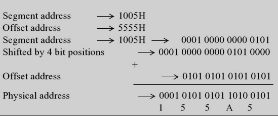
Memory addressing in the 8086 is segmented, meaning memory is divided into segments. To generate a physical memory address from segment and offset registers, each 16 bits long, the segment address is shifted left four times (equivalent to multiplying by 16) and added to the offset address. This combination produces a 20-bit physical address, allowing access to a large memory space.
For example, if the segment address is 1005H and the offset is 5555H, the physical address is calculated as follows:
- Segment Address: 1005H
- Offset Address: 5555H
- Physical Address: (1005H << 4) + 5555H = 10050H + 5555H = 15555H
This process enables the processor to access different parts of memory efficiently and manage large amounts of data effectively.
- Segmentation and Offset:
- Each segment, identified by a segment value like 1005H, can hold up to 64K memory locations (from 0000H to FFFFH).
- The segment register tells us where the segment starts, while the offset tells us the distance from the start to a specific memory location within that segment.
- Addressing Memory:
- To get the physical memory address, a special adder combines the segment’s base address with the offset.
- Depending on what you’re accessing (code, data, or stack), you use different segment registers. The offset can be from various sources like IP, BX, SI, etc.
- 8085 vs. 8086:
- In the 8085 processor, after fetching and decoding an instruction, the external bus remains idle while the processor executes the instruction internally.
- In the 8086 processor, this idle time is used to overlap the fetching of the next instruction. The fetched instructions are stored in a queue for decoding.
- Pipeline and Execution:
- The 8086 processor has a pipeline setup where fetching of the next instruction overlaps with the execution of the current one.
- The Bus Interface Unit (BIU) handles communication with memory and I/O devices, while the Execution Unit (EU) executes instructions.
- The BIU and EU work together, with the BIU managing memory and I/O operations under the timing and control unit’s direction.
- Components of Execution Unit:
- The Execution Unit contains registers for arithmetic and logic operations, a 16-bit ALU (Arithmetic Logic Unit), and a flag register reflecting ALU operation results.
- The decoding unit interprets instruction opcodes fetched from the queue, and the timing and control unit coordinates the execution based on the decoded instructions.
- Data Flow:
- Results from operations may be passed from the EU to the BIU for storage in memory.
In essence, the 8086 processor efficiently handles instruction execution by overlapping instruction fetching, decoding, and execution, utilizing its segmented memory architecture and a pipelined execution model.
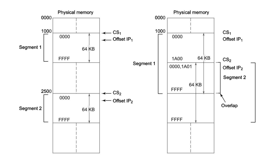
Memory Segmentation
In computers like the 8086/8088, memory is divided into segments. Each segment is like a section of memory, and each segment can hold up to 64K bytes of information. Think of it like dividing a big block of houses into smaller sections.
To find something in a segment, we use two pieces of information: the segment’s starting point and an offset, which tells us how far into the segment we need to go. Both of these pieces of information are 16 bits long, which means they can have values from 0000H to FFFFH.
To explain this idea, imagine a neighborhood with 100 houses. In one scenario, the houses are numbered sequentially from 1 to 100. If you want to find house number 67, you have to start from house 1 and count up until you reach 67.
Now, imagine those same 100 houses arranged in a grid, like a 10 by 10 grid of rows and columns. In this case, if you want to find house number 67, you just go to the 6th row and then to the 7th column. It’s much quicker and easier than counting sequentially.
This second scenario is similar to how segmented memory works. The segment address is like the row number, telling you which segment to look in, and the offset address is like the column number, telling you exactly where to find what you’re looking for. This segmented approach makes finding things in memory faster and more efficient.
The CPU 8086 can handle up to 1 megabyte (1Mbytes) of physical memory. This whole 1Mbytes can be split into 16 segments, each segment being 64Kbytes in size. These segments are numbered from 0000H to F000H.
Each segment can hold addresses ranging from 0000H to FFFFH, giving a total range of physical addresses from 00000H to FFFFFH.
In some cases, segments might overlap. This happens when one segment starts before another segment ends. The overlapping part is called the “overlapped segment area”. This means some memory locations can be addressed using two different combinations of segment and offset addresses.
The advantages of segmented memory are:
- It allows handling a large memory capacity (up to 1 megabyte) while using only 16-bit addresses.
- It enables separating code, data, and stack portions of a program into different memory segments for better protection.
- It allows programs to be placed in different parts of memory each time they’re run, which helps with relocation.
In the overlapped area, the physical address is formed by adding the Segment Register (CS) to either the Offset Register (JP) or the Instruction Pointer Register (IP).
Flag Register
The 8086 processor has a 16-bit flag register. This register is divided into two parts:
- Condition Code or Status Flags: This is the lower byte of the flag register, along with an additional overflow flag. These flags indicate the status of operations performed by the Arithmetic Logic Unit (ALU). They’re similar to the flag register in the 8085 processor, with the addition of the overflow flag.
- Machine Control Flags: This is the higher byte of the flag register. It includes three flags:
- Direction Flag (D): It determines the direction of certain operations, like string operations.
- Interrupt Flag (I): It controls the response to interrupt requests from external devices.
- Trap Flag (T): It’s used for debugging purposes to single-step through a program.
In simple terms, the flag register in the 8086 processor keeps track of the status of various operations and controls how the processor responds to interrupts and certain instructions.
- S-Sign Flag: This flag indicates whether the result of a computation is negative. For signed computations, it equals the Most Significant Bit (MSB) of the result.
- Z-Zero Flag: This flag is set if the result of the previous computation or comparison is zero.
- P-Parity Flag: Set to 1 if the lower byte of the result contains an even number of 1s.
- C-Carry Flag: Set when there’s a carry out of the Most Significant Bit (MSB) during addition, or a borrow during subtraction. For example, in addition, if a carry is generated from the highest bit position, this flag will be set to ‘1’. If no carry occurs, it will be ‘0’. Other instructions may also use or affect this flag.
- T-Trap Flag: When set, the processor enters single-step execution mode. After each instruction, a trap interrupt is generated, transferring control to the Trap interrupt service routine.
- I-Interrupt Flag: If set, the CPU recognizes maskable interrupts. If not set, it ignores them.
- D-Direction Flag: Used by string manipulation instructions. When ‘0’, strings are processed from lowest to highest address (auto-incrementing mode). When ‘1’, from highest to lowest address (auto-decrementing mode).
- AC-Auxiliary Carry Flag: Set if there’s a carry from the lowest nibble (bit 3) during addition, or a borrow for the lowest nibble during subtraction.
These flags provide crucial information about the status of operations and control how the processor responds to certain conditions and instructions.
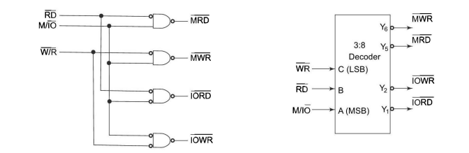
SIGNAL DESCRIPTIONS OF 8086
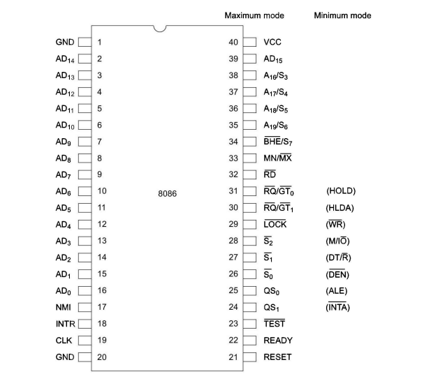
- Address/Data Bus (AD15-AD0): This is a bidirectional bus used for transferring addresses during the address phase of a bus cycle and data during the data phase. These lines carry the least significant 16 bits of memory addresses or data.
- Status Signals (S6-S3): These signals indicate the status of various operations during bus cycles.
- S6 (Status Bit 6): Used in conjunction with the S5 status signal to indicate the current bus cycle type.
- S5 (Status Bit 5): Used in conjunction with S6 to indicate the current bus cycle type.
- S4 (Status Bit 4): Indicates whether the current bus cycle is a memory or I/O operation.
- S3 (Status Bit 3): Indicates the direction of data flow during the current bus cycle.
- Control Signals (AEN, BHE, DEN, DT/R, HLDA, HOLD, LOCK, MN/MX, QS0, QS1, RESET, S0, S1, S2, TEST, WR, RD, INTR, INTA, READY, RESET, LOCK, NMI, SS0-SS1, SS0-SS3, LOCK, HLDA, MN/MX, QS0-QS1): These signals control various aspects of the processor’s operation, including memory and I/O access, interrupt handling, and bus arbitration.
- Power Supply (VCC, GND): VCC provides the processor’s power supply, while GND serves as the ground reference.
- Clock Signals (CLK, CLKOUT): CLK is the system clock input used to synchronize internal operations. CLKOUT is an output providing a buffered version of the processor’s clock.
- Test and Debugging Signals (TEST, RQ/GT1, RQ/GT0, TRST, TCLK): These signals facilitate testing and debugging of the processor.
- Mode Control Signals (M/IO, RD, WR, DEN, DT/R, HOLD, HLDA, RESET): These signals control the processor’s operating mode and bus cycles.
- Interrupt Signals (INTR, NMI, INTA, INT): These signals are used for handling interrupts from external devices.
- Address/Data Bus (AD15-AD0): These lines carry both address and data information. During the address phase of a bus cycle, they transmit memory addresses. During the data phase, they carry data to or from memory or I/O devices.
- Status Signals (S6-S3): These signals convey information about the current state of the processor during bus cycles:
- S6 (Status Bit 6) and S5 (Status Bit 5): Together, these signals indicate the current bus cycle type, such as memory read or write.
- S4 (Status Bit 4): Indicates whether the current bus cycle is accessing memory or an I/O device.
- S3 (Status Bit 3): Specifies the direction of data transfer during the current bus cycle, either read (from memory or I/O) or write (to memory or I/O).
- Control Signals: These signals control various aspects of the processor’s operation:
- AEN (Address Enable): Enables the address bus during memory operations.
- BHE (Bus High Enable): Enables the high byte of the data bus during memory or I/O operations.
- DEN (Data Enable): Enables the data bus during memory or I/O operations.
- DT/R (Data Transmit/Receive): Determines the direction of data transfer during memory or I/O operations.
- HLDA (Hold Acknowledge): Indicates that the processor has entered the Hold state in response to a Hold request.
- HOLD: A signal from an external device requesting control of the system bus.
- LOCK: Asserted during certain atomic operations to prevent bus access by other processors.
- MN/MX (Minimum/Maximum Mode): Selects the processor’s operating mode.
- QS0, QS1 (Queue Status): Indicates the status of the internal instruction queue.
- RESET: Resets the processor to a known state.
- S0-S2 (Status Bits 0-2): Together with S3-S6, these bits specify the current bus cycle type and processor status.
- TEST: Used for testing the processor during manufacturing.
- Power Supply (VCC, GND): VCC provides the processor’s supply voltage, while GND serves as the ground reference.
- Clock Signals (CLK, CLKOUT): CLK is the main clock input used to synchronize the processor’s operations. CLKOUT provides a buffered version of the system clock.
- Test and Debugging Signals (TEST, RQ/GT1, RQ/GT0, TRST, TCLK): These signals assist in testing and debugging the processor during development or troubleshooting.
- Mode Control Signals (M/IO, RD, WR, DEN, DT/R, HOLD, HLDA, RESET): These signals control the processor’s operating mode and bus cycles.
- Interrupt Signals (INTR, NMI, INTA, INT): These signals handle interrupts from external devices, allowing them to interrupt normal processor operation to request attention.
These signals play crucial roles in the operation of the 8086 processor, enabling communication with memory and I/O devices, managing interrupts, and controlling the processor’s behavior.
PHYSICAL MEMORY ORGANIZATION
- Address Space: Physical memory refers to the actual hardware memory cells in a computer system. It is organized as a linear array of memory cells, each uniquely identified by an address. The range of addresses represents the address space of the system, determining the maximum amount of memory the system can access.
- Memory Cells: Memory cells are the smallest units of storage in physical memory. Each memory cell typically stores one binary digit (bit) of information. In systems with byte-addressable memory, groups of memory cells are organized into bytes, with each byte containing 8 bits.
- Memory Organization:
- Byte Addressability: Memory is typically byte-addressable, meaning each memory cell has a unique address, and data can be read from or written to individual bytes.
- Word Size: Memory is often organized into words, which are groups of contiguous bytes that represent the native data size of the processor. For example, in a 32-bit system, a word may consist of 4 bytes (32 bits).
- Endianness: Memory organization may follow either big-endian or little-endian byte ordering, determining the order in which bytes are stored within a word.
- Memory Hierarchy:
- Primary Memory: Also known as main memory or RAM (Random Access Memory), primary memory stores data and instructions that are actively being used by the processor. It provides fast access to data but is volatile, meaning its contents are lost when the power is turned off.
- Secondary Memory: Secondary memory, such as hard disk drives (HDDs) and solid-state drives (SSDs), provides long-term storage for data and programs. It is non-volatile and retains data even when the power is off but typically has slower access times compared to primary memory.
- Cache Memory: Cache memory sits between the processor and main memory, storing frequently accessed data and instructions to reduce access times. It operates at a higher speed than main memory but has a smaller capacity.
- Memory Mapping:
- Physical Address Space: The actual addresses used to access memory cells in hardware.
- Virtual Address Space: The range of addresses visible to software programs, which may be mapped to physical memory addresses by the operating system.
- Memory Protection: Systems may implement memory protection mechanisms to prevent unauthorized access to memory regions. This can include read-only memory areas, memory segmentation, and memory paging.
- Memory Management Units (MMUs): MMUs are hardware components responsible for translating virtual addresses generated by the processor into physical memory addresses. They also handle memory protection and access control.
- Memory Interfacing: Memory is interfaced with the processor and other system components via buses, which provide the pathways for data transfer between memory and other devices.
GENERAL BUS OPERATION
- Introduction to Buses:
- In computer architecture, a bus is a communication pathway that allows different components of a computer system to exchange data and control signals.
- Buses can be classified based on their purpose, such as address buses, data buses, and control buses.
- Types of Buses:
- Address Bus: Transmits memory addresses generated by the CPU or other devices. The width of the address bus determines the maximum addressable memory space.
- Data Bus: Carries data between the CPU, memory, and I/O devices. The width of the data bus determines the number of bits that can be transferred simultaneously.
- Control Bus: Carries control signals that coordinate the operation of devices connected to the bus. Control signals include read, write, and interrupt signals.
- Bus Operation:
- Bus Cycle: A bus cycle refers to the sequence of actions involved in transferring data or control signals over the bus.
- Address Phase: In the address phase, the CPU places the memory address or I/O port address on the address bus. This address specifies the source or destination of data transfer.
- Data Phase: In the data phase, data is transferred over the data bus between the CPU and memory or I/O devices. The direction of data transfer is controlled by signals on the control bus, such as read and write signals.
- Control Phase: The control phase includes signals that control the timing and synchronization of bus operations. These signals ensure that data is transferred correctly and that devices are enabled or disabled at the appropriate times.
- Bus Arbitration:
- In systems with multiple devices connected to the bus, bus arbitration is used to determine which device has access to the bus at any given time.
- Techniques such as priority-based arbitration and time-based arbitration are used to resolve conflicts and allocate bus access to different devices.
- Synchronous vs. Asynchronous Bus Operation:
- Synchronous Bus: In a synchronous bus, data transfers are synchronized with a clock signal. Each bus cycle occurs within a fixed time frame determined by the clock frequency.
- Asynchronous Bus: In an asynchronous bus, data transfers occur without a fixed time reference. Devices communicate using handshaking signals to indicate when data is ready to be transferred.
- Bus Protocols:
- Various bus protocols define the rules and procedures for communication over the bus. Examples include the Peripheral Component Interconnect (PCI), Universal Serial Bus (USB), and Inter-Integrated Circuit (I2C) protocols.
- Bus Performance:
- Bus performance is influenced by factors such as bus width, clock frequency, and the number of devices connected to the bus. Increasing bus width and clock frequency can improve data transfer rates, while adding more devices may increase bus contention and reduce performance.
I/O ADDRESSING CAPABILITY
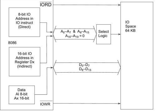
The 8086/8088 processor has the capability to address up to 64K I/O byte registers or 32K word registers. However, there’s a limitation: the address of an I/O device must not exceed 16 bits in size. This restriction means that the CPU can access a maximum of 2^16, or 64Kbyte, I/O devices.
During an I/O operation, the I/O address is presented on the address lines A0 to A15 for one clock cycle (T1). To ensure accurate address reception, the address can then be latched using the Address Latch Enable (ALE) signal. Additionally, the upper address lines (A16 to A19) are held at logic 0 level during I/O operations.
The 16-bit register DX serves as a 16-bit I/O address pointer, allowing for the full capability to address up to 64K devices. In this setup, the I/O ports are addressed similarly to memory locations in the base addressing mode, utilizing the BX register.
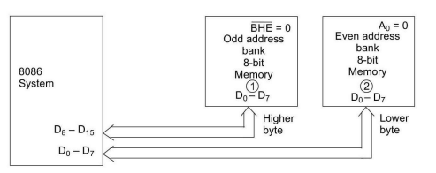
In memory-mapped I/O interfacing, the I/O device addresses are treated as memory locations in page 0, which corresponds to the segment address 0000H. This means that even-addressed bytes are transferred on the D0 to D7 lines, while odd-addressed bytes are transferred on the D8 to D15 lines.
When designing an 8-bit I/O system around the 8086 processor, it’s crucial to ensure that all byte registers in the system are even addressed. This is important for maintaining compatibility and proper data transfer.
SPECIAL PROCESSOR ACTIVITIES
Special processor activities refer to tasks that are performed by processors other than the main central processing unit (CPU). These processors are designed to handle specific tasks more efficiently than the CPU can on its own. Some common examples of special processor activities include:
- Floating-point unit (FPU): An FPU is a coprocessor that is designed to perform floating-point arithmetic operations. Floating-point numbers are used to represent real numbers that cannot be accurately represented using integers. FPUs are essential for applications that require high precision calculations, such as scientific computing, engineering, and graphics.
- Vector processor: A vector processor is a type of processor that can perform operations on multiple data elements simultaneously. This makes vector processors well-suited for applications that involve large amounts of data, such as image processing, video processing, and signal processing.
- Graphics processing unit (GPU): A GPU is a specialized processor that is designed to accelerate the creation of images and video. GPUs are commonly used in graphics cards, game consoles, and other devices that require high-performance graphics processing.
- Digital signal processor (DSP): A DSP is a type of processor that is designed to process digital signals. DSPs are commonly used in applications such as audio processing, telecommunications, and industrial control.
- Application-specific integrated circuit (ASIC): An ASIC is a chip that is designed for a specific application. ASICs can be used to implement special processor activities that are not available on standard processors.
- Special processor activities can improve the performance of a computer system by offloading tasks from the CPU. This can be especially beneficial for applications that require a lot of processing power.
Processor Reset and Initialization
When you set the RESET pin to a high signal, it resets the microprocessor. It stays reset until you set the pin back to a low signal. When this happens with the 8086 microprocessor, any ongoing operation stops as soon as the reset signal goes from low to high. When it goes from high to low, the reset sequence begins and lasts for about 10 clock cycles. During this time, all the internal registers are set to zero, except for the CS register, which is set to FFFFH. This means that the execution restarts from the physical memory address FFFFOH. To accommodate this, the EPROM in an 8086 system is arranged to have memory locations from FFFFOH to FFFFFH at the end of the memory map.
For the 8086 to recognize the reset signal, it needs to be high for at least 4 clock cycles. After turning on the power, you shouldn’t apply the reset pulse to the 8086 for at least 50 microseconds to ensure proper initialization.
During the reset state, all outputs that can be in a high-impedance state are set to that state. Certain status signals are active briefly when the reset first happens, then they go into a high-impedance state. Two specific lines, ALE and HLDA, are set to low during the reset operation.
If a non-maskable interrupt request happens before the second clock cycle after the reset finishes, it won’t be responded to. For the NMI request to be recognized, it needs to occur after the second clock cycle during the reset initialization or later. If a HOLD request comes in immediately after a reset, it will be attended to right after initialization, before any instructions are executed.
Understanding the Significance:
- Impact on Program Execution: Explain how the reset sequence disrupts ongoing operations and ensures a controlled program restart. Highlight the importance of code residing at FFFFOH to handle initialization after reset.
- Hardware Design Choices: Discuss the rationale behind placing reset-related memory in EPROM (Read-Only Memory) and the advantages of tristate outputs during reset.
- Timing Constraints: Emphasize the crucial role of minimum reset pulse duration (4 clock cycles) and power-on initialization delay (50 μs) for stable operation.
2. Practical Applications:
- Debugging: Point out how understanding the reset sequence can aid in debugging issues that arise during power-on or reset situations.
- Interrupt Handling: Explain how NMI requests differ from other interrupts during reset and when they become active.
- System Design: Connect the reset sequence to broader system design considerations, such as power sequencing and external reset circuitry.
3. Additional Insights:
- Modern Processors: Briefly compare and contrast the reset behavior of the 8086 with modern processors, like those used in personal computers.
- Future Advancements: Discuss potential future trends in reset sequences and their impact on system design and performance.
HALT
When the processor gets a command to stop (HLT), it goes into a standby mode. But, before doing that, it lets the system know it’s entering standby in two different ways, depending on whether it’s in basic mode or advanced mode.
In basic mode, it sends a signal without any extra commands. In advanced mode, it sends a specific signal and then a pulse, but without sending any extra commands.
While in standby, the processor won’t respond to regular commands. It needs an interrupt or reset to start working again. Even a request to hold the processor won’t bring it out of standby.
TEST and Synchronisation with External Signals
In addition to its regular functions like handling interrupts and I/O operations, the 8086 processor also has a feature called the TEST signal.
When the CPU encounters a WAIT instruction, it stops what it’s doing and holds onto the data in its registers. It then waits for a signal called TEST to drop to a low level. If TEST does go low, the CPU continues with its tasks. But if TEST stays high, the CPU keeps waiting until TEST goes low. For the TEST signal to be recognized, it has to stay low for at least 5 clock cycles.
While waiting, the CPU doesn’t use up any processing cycles. It just sits idle. However, it can still respond to requests from external devices to pause its operations (like a HOLD request).
If an interrupt happens while the CPU is waiting, it repeats the WAIT instruction, handles the interrupt, and then goes back to waiting. This way, the program can sync up with an external signal connected to the TEST pin.
In simpler terms, the WAIT instruction lets the CPU pause until a certain signal (TEST) goes low, allowing for synchronization with external events.
Deriving System Bus
Deriving the system bus in a microprocessor involves the design and implementation of the pathway through which data, addresses, and control signals travel between the processor and other components within the system.
Here are the key steps and considerations in deriving the system bus:
- Understanding System Requirements: The first step is to understand the requirements of the system, including the types of components that need to communicate with the microprocessor, such as memory, input/output devices, and other peripherals.
- Bus Width: Determine the width of the system bus, which refers to the number of lines or wires used for data transfer. This is typically expressed in bits (e.g., 8-bit, 16-bit, 32-bit, etc.) and affects the maximum amount of data that can be transferred in a single cycle.
- Addressing: Define the addressing scheme for memory and I/O devices. This includes determining the range of addresses that the microprocessor can access and how these addresses are mapped to specific memory locations or device registers.
- Control Signals: Identify and define the control signals needed for communication on the system bus. These signals include read/write signals, bus enable signals, clock signals, and various handshaking signals to manage data transfer and synchronization between components.
- Timing Considerations: Establish timing requirements for the bus, including signal propagation delays, setup and hold times, and clock frequencies. Ensuring proper timing is crucial for reliable data transfer and system operation.
- Bus Arbitration: If the system includes multiple devices that need access to the bus, implement a bus arbitration mechanism to manage access conflicts and determine which device can use the bus at any given time. Common arbitration methods include priority-based, round-robin, and token passing schemes.
- Electrical Characteristics: Consider the electrical characteristics of the bus, such as voltage levels, signal integrity, and termination methods, to ensure reliable communication and compatibility with connected components.
- Physical Implementation: Design the physical connections for the system bus, including the layout of traces on the printed circuit board (PCB) and the selection of connectors and termination components.
- Testing and Verification: Thoroughly test and verify the functionality of the system bus through simulation, prototyping, and testing with real hardware. This includes checking for data integrity, timing accuracy, and compatibility with different devices and configurations.
- Documentation: Document the specifications and implementation details of the system bus, including pin assignments, signal descriptions, timing diagrams, and any relevant design considerations. This documentation is essential for understanding and maintaining the system architecture.
By following these steps and considerations, designers can derive a robust and efficient system bus for microprocessor-based systems, enabling seamless communication between the processor and other system components.
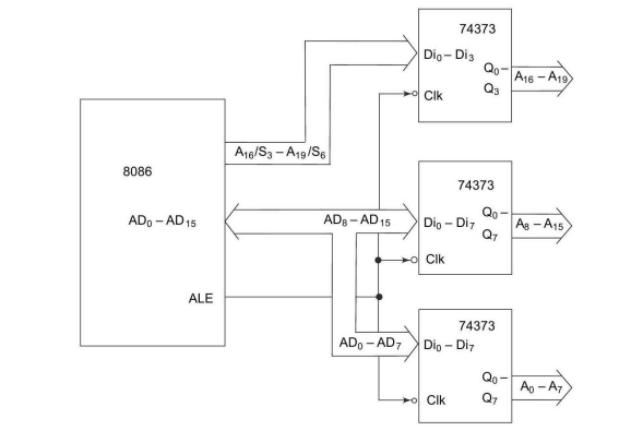
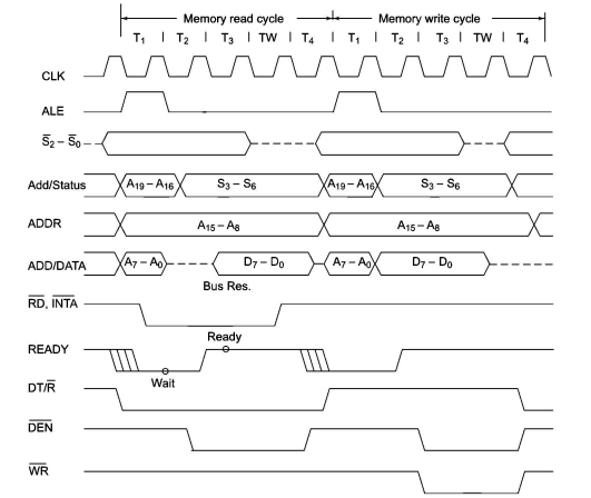
MINIMUM MODE 8086 SYSTEM AND TIMINGS
Creating a minimum mode 8086 system involves configuring the microprocessor to operate in a basic mode where it communicates directly with memory and I/O devices without the assistance of additional support chips. Here’s a comprehensive guide covering the setup and timings of a minimum mode 8086 system:
A. Architecture Overview:
- 8086 Microprocessor: The central processing unit (CPU) of the system, responsible for executing instructions and performing data processing tasks.
- Memory: Both random access memory (RAM) and read-only memory (ROM) are used to store program instructions and data.
- I/O Devices: Input/output devices such as keyboards, displays, and storage devices are connected to the system for data input and output.
- Minimum Mode Operation: The 8086 microprocessor operates in minimum mode when it directly communicates with memory and I/O devices without additional support chips like the 8288 bus controller.
B. System Components:
- 8086 Microprocessor: The heart of the system, executing instructions fetched from memory and controlling data flow between memory and I/O devices.
- Memory Chips: RAM and ROM chips provide storage for program instructions and data. Memory chips are interfaced with the microprocessor through the address bus, data bus, and control signals.
- I/O Devices: Various input and output devices are connected to the system, requiring appropriate interfacing with the microprocessor for data exchange.
C. System Configuration:
- Address Bus: The 8086 microprocessor has a 20-bit address bus, allowing access to a maximum of 1 MB of memory.
- Data Bus: The 8086 microprocessor has a 16-bit data bus for transferring data between the processor and memory or I/O devices.
- Control Signals: Control signals such as read, write, address latch enable (ALE), and memory/IO are used to control the flow of data and addresses between the microprocessor and external devices.
D. Timings in Minimum Mode:
- Machine Cycle: A basic unit of time during which the 8086 microprocessor performs one operation. The machine cycle consists of several clock cycles.
- Clock Frequency: The frequency at which the system clock pulses, typically measured in megahertz (MHz). The 8086 microprocessor operates with a clock frequency ranging from 5 to 10 MHz.
- Instruction Execution Time: The time taken by the microprocessor to execute a single instruction, determined by factors such as instruction complexity and memory access time.
- Memory Access Time: The time taken to access data from memory, including the time for address generation, memory access, and data retrieval.
- I/O Device Access Time: The time taken to transfer data between the microprocessor and I/O devices, including any necessary handshaking or synchronization.
- Bus Timings: Timings related to bus operations, including address setup time, address hold time, data setup time, and data hold time, ensure proper data transfer and synchronization between the microprocessor and external devices.
E. System Operation:
- Instruction Fetch: The microprocessor fetches instructions from memory using the address bus and data bus.
- Instruction Decode and Execute: The fetched instruction is decoded and executed by the microprocessor, which may involve accessing data from memory or performing arithmetic or logical operations.
- Data Transfer: Data is transferred between the microprocessor and memory or I/O devices as required by the executed instructions.
- Interrupt Handling: The microprocessor responds to interrupt requests from external devices by suspending the current execution and transferring control to the interrupt service routine.
F. System Interfacing:
- Memory Interfacing: Memory chips are connected to the microprocessor through the address bus, data bus, and control signals, allowing the microprocessor to read from and write to memory locations.
- I/O Device Interfacing: Input and output devices are connected to the microprocessor through appropriate interface circuits, allowing data exchange between the microprocessor and external devices.
- Interrupt Handling: Interrupt signals from external devices are connected to the microprocessor, allowing the microprocessor to respond to external events such as timer expiration or I/O device status changes.
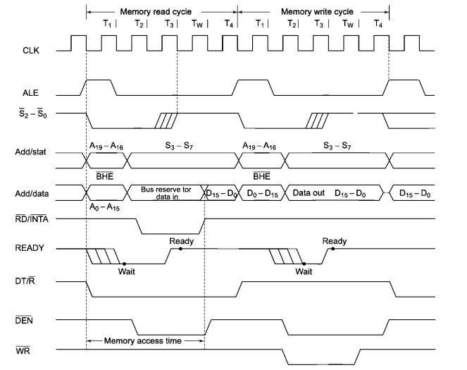
G. System Timing Diagrams:
- Address Timing Diagram: Illustrates the timing relationships between address signals and clock pulses during memory access operations.
- Data Timing Diagram: Shows the timing relationships between data signals and clock pulses during data transfer operations.
- Control Timing Diagram: Depicts the timing relationships between control signals and clock pulses during various bus operations.
By following these steps and considerations, a minimum mode 8086 system can be configured and operated efficiently, with proper attention to timings and interfacing requirements.
Timings for RQ/GT Signals
Timings for RQ/GT signals in a microprocessor system refer to the timing characteristics and considerations associated with the Request (RQ) and Grant (GT) signals used for bus arbitration. Here’s a comprehensive overview from A to Z:
A. Arbitration Scheme:
- Request (RQ) Signal: Generated by a device requesting access to the system bus.
- Grant (GT) Signal: Issued by the bus arbiter to grant access to a requesting device.
B. Bus Arbitration Process:
- Request Generation: Devices in need of bus access assert the RQ signal.
- Arbitration: The bus arbiter prioritizes and grants access to devices based on predefined criteria.
- Grant Issuance: The arbiter selects a device and asserts the GT signal, indicating permission to use the bus.
C. Clocking Signals:
- System Clock: The timing reference for all bus operations and signals, including RQ/GT.
- Clock Edge: Transition points on the clock signal used for synchronizing the timing of RQ/GT signals.
D. Delay Considerations:
- Propagation Delay: The time taken for RQ/GT signals to propagate through the bus arbitration logic.
- Setup Time: The minimum time before the active edge of the clock when the RQ signal must be stable and valid.
- Hold Time: The minimum time after the active edge of the clock when the RQ signal must remain valid.
E. Error Handling:
- Timeout Mechanism: If a device does not receive a GT signal within a specified time window, it may initiate error handling routines.
- Retry Mechanism: Devices may retry the arbitration process if their RQ signals are not granted within a certain timeframe.
F. Frequency Considerations:
- Clock Frequency: The rate at which the system clock oscillates, influencing the timing of RQ/GT signals.
- Bus Bandwidth: Higher clock frequencies may lead to tighter timing constraints for RQ/GT signals due to faster bus cycles.
G. Generation of RQ/GT Signals:
- Device Request: Devices assert the RQ signal when they require access to the bus.
- Arbiter Decision: The bus arbiter examines all active RQ signals and selects one device to grant access by asserting the GT signal.
H. Handshaking Protocol:
- Request-Acknowledge Protocol: Devices acknowledge the receipt of GT signals upon being granted bus access.
- Error Signaling: Devices may signal errors or contention issues if RQ/GT signals are not properly synchronized or honored.
I. Interfacing Requirements:
- Electrical Characteristics: RQ/GT signals must meet specified voltage levels, noise margins, and slew rates for reliable operation.
- Termination: Proper termination techniques may be employed to minimize signal reflections and ensure signal integrity.
J. Jitter Analysis:
- Clock Jitter: Variations in the timing of clock edges may impact the stability and accuracy of RQ/GT signal timing.
- Signal Skew: Timing mismatches between RQ and GT signals due to differences in signal propagation paths may introduce jitter.
K. Kinetics of Bus Access:
- Priority Assignment: Devices may be assigned different priority levels for bus access, affecting the timing and order of RQ/GT signal transactions.
- Latency: The time between a device’s RQ signal assertion and the receipt of a GT signal determines the delay before actual bus access.
L. Latency Analysis:
- Arbiter Response Time: The time taken by the arbiter to select a device and assert the corresponding GT signal.
- Bus Occupancy Time: The duration for which a device holds control of the bus after being granted access by the GT signal.
M. Memory Access Timings:
- Read/Write Cycle: The timing constraints associated with memory read and write operations, which may be affected by RQ/GT signal latency.
- Bus Turnaround Time: The time required for the bus to transition from a read to a write operation or vice versa, impacting overall memory access timings.
N. Negotiation Protocol:
- Bus Protocol Compliance: Devices must adhere to the specified bus protocol for proper generation and interpretation of RQ/GT signals.
- Conflict Resolution: Arbitration algorithms and protocols ensure fair and efficient resolution of bus access conflicts among multiple requesting devices.
O. Operational Modes:
- Synchronous Mode: RQ/GT signals are synchronized with the system clock, allowing for precise timing control and coordination.
- Asynchronous Mode: RQ/GT signals may operate independently of the system clock, introducing additional timing uncertainty and complexity.
P. Protocol Verification:
- Functional Testing: Verification of RQ/GT signal timing through simulation or emulation of bus arbitration scenarios.
- Timing Analysis: Formal analysis techniques may be employed to ensure that RQ/GT signal timing requirements are met under all operating conditions.
Q. Quality of Service (QoS):
- Bus Priority Levels: Devices with higher priority levels may be granted access to the bus more quickly, reducing latency for critical operations.
- Service Guarantees: The system may provide guarantees regarding the maximum latency or response time for RQ/GT signal transactions to meet QoS requirements.
R. Reliability Considerations:
- Error Detection: Mechanisms for detecting and handling errors in RQ/GT signal transactions to ensure the reliability of bus access.
- Redundancy: Duplication of critical components or signals may be employed to enhance the reliability of RQ/GT signal processing and arbitration.
S. System-Level Integration:
- Bus Interface Units: Hardware modules responsible for generating and interpreting RQ/GT signals and interfacing with the bus arbiter.
- Integration Testing: Verification of RQ/GT signal timing and behavior in the context of the overall system architecture, including interactions with other subsystems and devices.
T. Timing Diagrams:
- RQ Signal Timing: Illustrates the timing relationships between RQ signal assertion, arbitration, and GT signal issuance.
- GT Signal Timing: Depicts the timing characteristics of GT signal assertion and its relationship with RQ signals and bus access transactions.
U. User-Defined Timing Parameters:
- Configurability: Some aspects of RQ/GT signal timing may be configurable or programmable to accommodate varying system requirements.
- Customization: System designers may define specific timing parameters or constraints for RQ/GT signal transactions based on application-specific considerations.
V. Verification and Validation:
- Timing Simulation: Simulation of RQ/GT signal transactions and bus arbitration scenarios to verify compliance with specified timing requirements.
- Validation Testing: Experimental validation of RQ/GT signal timing through hardware testing and measurement under real-world operating conditions.
W. Wait States:
- Insertion of Wait States: In cases where RQ/GT signal timing cannot be met, the system may insert additional wait states to accommodate slower devices or bus access transactions.
- Impact on Performance: The insertion of wait states may increase overall bus access latency and degrade system performance, necessitating careful optimization of RQ/GT signal timing.
X. Xilinx FPGA Implementation:
- FPGA-Based Bus Arbiter: Utilization of Xilinx FPGAs for implementing custom bus arbitration logic and processing RQ/GT signals.
- Timing Constraints: Consideration of FPGA-specific timing constraints and limitations in the design and implementation of RQ/GT signal processing logic.
Y. Yield Analysis:
- Manufacturing Variability: Analysis of RQ/GT signal timing variability due to manufacturing process variations and device-specific characteristics.
- Yield Optimization: Techniques for optimizing RQ/GT signal timing to maximize manufacturing yield and ensure consistent performance across device populations.
Z. Zero-Delay Buffers:
- Signal Skew Reduction: Utilization of zero-delay buffers to minimize signal skew and ensure precise synchronization of RQ/GT signals with the system clock.
- Timing Alignment: Zero-delay buffers may be employed to align the timing of RQ/GT signals with other critical signals in the system, facilitating accurate bus arbitration and data transfer operations.
By considering these aspects from A to Z, designers can effectively manage the timing characteristics of RQ/GT signals in a microprocessor system, ensuring reliable and efficient bus arbitration and data transfer operations.
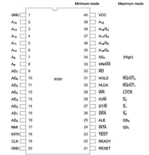
THE PROCESSOR 8088
The Intel 8088 microprocessor, released in 1979, is a variant of the widely used 8086 processor. Here’s a comprehensive guide covering the details of the 8088 processor from A to Z:
A. Architecture Overview:
- 16-bit Processor: The 8088 is a 16-bit microprocessor, meaning it operates on 16-bit data and addresses.
- x86 Architecture: It belongs to the x86 family of processors, which has been the basis for most desktop and laptop processors since its inception.
- Registers: The 8088 has several registers, including general-purpose registers (AX, BX, CX, DX), index registers (SI, DI), and segment registers (CS, DS, SS, ES).
B. Bus Interface:
- 8-bit Data Bus: Unlike the 8086, which has a 16-bit data bus, the 8088 has an 8-bit data bus.
- 20-bit Address Bus: Similar to the 8086, the 8088 has a 20-bit address bus, allowing it to access up to 1 MB of memory.
C. Clock Speed:
- Clock Frequency: The 8088 operates at a clock frequency of 4.77 MHz in most systems. However, it can also be operated at higher frequencies.
- External Clock Signal: The processor synchronizes its operations with an external clock signal provided by the system.
D. Data Movement Instructions:
- MOV: Used to move data between registers, memory, and I/O devices.
- XCHG: Exchanges the contents of two registers or a register and a memory location.
- PUSH and POP: Used to push data onto the stack or pop data from the stack, respectively.
E. Execution Unit:
- ALU (Arithmetic Logic Unit): Performs arithmetic and logic operations such as addition, subtraction, AND, OR, etc.
- Instruction Execution: Executes instructions fetched from memory or external devices.
F. Flags Register:
- Status Flags: The 8088 has several status flags in the FLAGS register, including carry flag (CF), zero flag (ZF), sign flag (SF), overflow flag (OF), and others.
- Flag Manipulation: Instructions such as CMP, TEST, and logical instructions modify these flags based on the result of the operation.
G. General-Purpose Registers:
- AX, BX, CX, DX: These are 16-bit general-purpose registers used for various arithmetic and data manipulation operations.
- Index Registers (SI, DI): Used for pointer manipulation in string operations and memory access.
H. Hardware Interrupts:
- Interrupt Handling: The 8088 supports hardware interrupts, allowing external devices to interrupt the processor’s normal execution flow.
- Interrupt Vector Table: Contains addresses of interrupt service routines (ISRs) for different interrupt types.
I. Instruction Set:
- x86 Instruction Set: The 8088 supports a rich instruction set comprising arithmetic, logical, data movement, control transfer, and string manipulation instructions.
- Compatibility: Most of the instructions are backward compatible with previous Intel processors, facilitating software compatibility.
J. Jump Instructions:
- JMP: Unconditional jump to a specified memory location or label.
- Jcc: Conditional jump instructions based on the state of the flags register (e.g., JE, JNE, JG, JL).
K. Key Features:
- Segmented Memory Model: Like the 8086, the 8088 uses a segmented memory model, dividing memory into segments and offsets.
- Peripheral Interface: Supports interfacing with various peripherals and I/O devices such as keyboards, displays, and storage devices.
L. Logical Instructions:
- AND, OR, XOR: Perform bitwise logical operations between operands.
- NOT: Performs bitwise negation of the operand.
M. Memory Management:
- Segmentation: Memory is divided into segments of up to 64 KB each, addressed using segment registers.
- Segment Offset Addressing: Memory addresses are calculated by combining a segment value with an offset value.
N. Numeric Coprocessor Support:
- 8087 Coprocessor: The 8088 can be used with the optional 8087 numeric coprocessor for hardware acceleration of floating-point arithmetic operations.
- FPU Instructions: The 8088 supports special instructions for interfacing with the 8087 coprocessor.
O. Operand Size:
- 8-bit and 16-bit Data: The 8088 can operate on both 8-bit and 16-bit data.
- Operand Size Prefix: Instructions can be prefixed with an operand size override prefix to specify the size of the operand.
P. Pipelining:
- Instruction Pipeline: The 8088 employs a simple instruction pipeline, allowing it to fetch the next instruction while executing the current one.
- Single-Stage Pipeline: Unlike modern processors, the 8088 has a single-stage pipeline, which limits its instruction throughput.
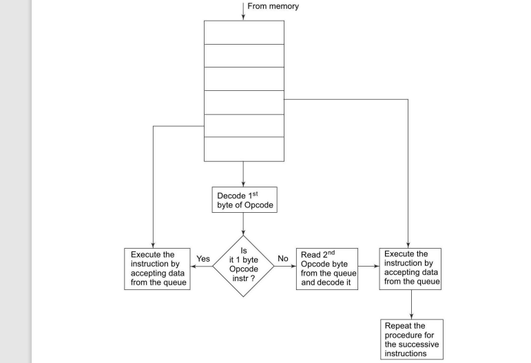
Q. Queue Management:
- Instruction Queue: The processor has a small internal queue to store prefetched instructions, helping to improve instruction fetch bandwidth.
- Queue Size: The size of the instruction queue is limited, typically holding a few instructions at a time.
R. Real Mode Operation:
- Real Address Mode: The 8088 operates in real mode by default, providing backward compatibility with older software.
- Flat Memory Model: In real mode, the processor uses a flat memory model, treating all memory addresses as physical addresses.
S. Stack Operations:
- PUSH and POP: Used for stack operations, pushing data onto the stack or popping data from the stack.
- Stack Pointer (SP): Points to the current top of the stack, used for managing the stack.
T. Timing Diagrams:
- Clock Timing: Illustrates the timing relationships between the clock signal and various internal operations of the processor.
- Bus Timing: Depicts the timing characteristics of bus transactions, including memory read/write cycles and I/O operations.
U. Unconditional Branches:
- CALL: Calls a subroutine by pushing the current instruction pointer onto the stack and transferring control to the specified address.
- RET: Returns from a subroutine by popping the return address from the stack and transferring control back to it.
V. Vector Processing:
- Interrupt Vector Table: Contains addresses of interrupt service routines (ISRs) for handling hardware interrupts.
- Interrupt Priority: Different interrupt types have different priorities, determined by their position in the interrupt vector table.
W. Wait States:
- Insertion of Wait States: In certain situations, the processor may insert wait states to synchronize with slower external devices or memory.
- Impact on Performance: Wait states increase the effective access time and may reduce the overall performance of the system.
X. X86 Compatibility:
- Backward Compatibility: The 8088 is backward compatible with previous Intel processors, ensuring compatibility with existing software.
- Legacy Support: Many modern x86 processors still support legacy instructions and modes for backward compatibility with older software.
Y. Yield Analysis:
- Manufacturing Yield: Analysis of manufacturing yield and defect rates to ensure reliable production of 8088 processors.
- Process Optimization: Yield analysis informs process optimization efforts to improve manufacturing efficiency and reduce defects.
Z. Zero Flag:
- ZF Flag: A status flag in the FLAGS register indicating whether the result of an arithmetic or logical operation is zero.
- Conditional Branching: Instructions such as JE (Jump if Equal) and JZ (Jump if Zero) use the ZF flag to conditionally branch based on the result of a comparison.
By understanding the architecture, features, and operation of the Intel 8088 microprocessor, developers can effectively design and program systems based on this iconic processor.
Architecture and Signal Description of 8088
The architecture and signal description of the Intel 8088 microprocessor provide insights into its internal structure, operation, and communication with external devices. Here’s a comprehensive guide from A to Z:
A. Address Bus (AD[19:0]):
- Description: The 20-bit address bus provides memory addresses for accessing up to 1 MB of memory.
- Usage: Used to select memory locations and I/O ports during read and write operations.
B. Bus Control Signals:
- Description: Signals used to control bus operations, including read, write, and various control functions.
- Examples: RD (Read), WR (Write), DT/R (Data Transmit/Receive), DEN (Data Enable), ALE (Address Latch Enable).
C. Clock Signal (CLK):
- Description: The clock signal provides timing synchronization for internal operations and external communication.
- Usage: All internal operations and external interactions are synchronized with the rising and falling edges of the clock signal.
D. Data Bus (D[7:0]):
- Description: The 8-bit data bus facilitates the transfer of data between the microprocessor and external devices.
- Usage: Data is transmitted bidirectionally on the data bus during read and write operations.
E. Execution Unit:
- Description: The execution unit interprets and executes instructions fetched from memory or external devices.
- Functions: Includes the Arithmetic Logic Unit (ALU) for performing arithmetic and logical operations, control unit for instruction decoding and execution, and register set for storing data and operands.
F. Flags Register (FLAGS):
- Description: A register containing various status flags that reflect the outcome of arithmetic and logical operations.
- Flags: Includes the Carry flag (CF), Zero flag (ZF), Sign flag (SF), Overflow flag (OF), and others, which indicate different conditions and results of operations.
G. General-Purpose Registers:
- Description: Registers used for general data storage and manipulation within the microprocessor.
- Registers: Includes AX, BX, CX, DX, SI, DI, BP, and SP, each with specific roles and functions in instruction execution and data processing.
H. Hold/Hold Acknowledge (HOLD, HLDA):
- Description: Signals used in bus arbitration to temporarily suspend the microprocessor’s activities and relinquish control of the system bus.
- Usage: When the microprocessor receives a HOLD signal, it responds by asserting the HLDA signal to indicate that it has entered a hold state.
I. Interrupts and Interrupt Control Signals:
- Description: Interrupts are signals used to temporarily suspend the execution of the current program and handle external events.
- Signals: Includes INTA (Interrupt Acknowledge), INTR (Interrupt Request), NMI (Non-Maskable Interrupt), and others for managing interrupt processing.
J. Jump Instructions:
- Description: Instructions used for altering the flow of program execution by jumping to different memory locations.
- Examples: JMP (Unconditional Jump), JZ/JNZ (Jump if Zero/Not Zero), JC/JNC (Jump if Carry/No Carry), and others.
K. Keyboard/Display Interface:
- Description: Interfaces for connecting external devices such as keyboards and displays to the microprocessor.
- Communication: Data is exchanged between the microprocessor and these devices using specific protocols and communication methods.
L. Logic Instructions:
- Description: Instructions for performing logical operations such as AND, OR, XOR, and NOT.
- Usage: Used for bitwise manipulation of data and control flow in program execution.
M. Memory Management Unit (MMU):
- Description: The MMU manages memory access and translation between logical addresses and physical addresses.
- Functions: Translates segment+offset addresses into physical addresses, enforces memory protection, and handles memory segmentation.
N. Numeric Coprocessor Interface:
- Description: Interface for connecting an optional numeric coprocessor, such as the Intel 8087, to the microprocessor.
- Functionality: Offloads floating-point arithmetic operations to the coprocessor for improved performance in mathematical calculations.
O. Opcode Fetch Unit:
- Description: The opcode fetch unit retrieves instructions from memory or external devices for execution.
- Operation: Fetches instructions based on the address provided by the instruction pointer (IP) register and prepares them for decoding and execution.
P. Power Supply and Reset Signals:
- Description: Signals for supplying power to the microprocessor and resetting its internal state.
- Examples: VCC (Power Supply Voltage), GND (Ground), RESET (Reset Signal), READY (Ready Signal).
Q. Queue Management:
- Description: Management of instruction and data queues within the microprocessor for efficient processing.
- Functions: Optimizes instruction execution by prefetching and buffering instructions, reducing pipeline stalls and latency.
R. Read/Write Control Signals:
- Description: Signals used to control read and write operations on the system bus.
- Examples: RD (Read), WR (Write), DT/R (Data Transmit/Receive), DEN (Data Enable).
S. Stack Pointer (SP) and Stack Operations:
- Description: The stack pointer register points to the top of the stack, used for managing subroutine calls, parameter passing, and local variable storage.
- Operations: PUSH (Push Data onto Stack), POP (Pop Data from Stack), CALL (Call Subroutine), RET (Return from Subroutine).
T. Timing Diagrams:
- Description: Diagrams illustrating the timing relationships between different signals and operations within the microprocessor.
- Examples: Clock timing diagrams, bus timing diagrams, instruction execution timing diagrams.
U. Unconditional Branches:
- Description: Instructions used for altering the program flow unconditionally, regardless of specific conditions or flags.
- Examples: JMP (Unconditional Jump), CALL (Call Subroutine), RET (Return from Subroutine).
V. Vector Processing:
- Description: Processing of interrupt vectors and handling of interrupt requests from external devices.
- Functions: Interrupt vectors point to specific locations in memory where interrupt service routines (ISRs) are located for handling external events.
W. Wait States:
- Description: Insertion of wait states to synchronize operations with slower external devices or memory.
- Purpose: Ensures proper timing alignment and data integrity during bus transactions and memory accesses.
X. x86 Instruction Set:
- Description: The 8088 supports a rich instruction set comprising arithmetic, logical, data movement, control transfer, and string manipulation instructions.
- Compatibility: Most instructions are backward compatible with previous Intel processors, facilitating software compatibility and migration.
Y. Yield Analysis:
- Description: Analysis of manufacturing yield and defect rates to ensure reliable production of 8088 microprocessors.
- Optimization: Yield analysis informs process optimization efforts to improve manufacturing efficiency and reduce defects.
Z. Zero Flag (ZF) and Conditional Branching:
- Description: The Zero flag indicates whether the result of an arithmetic or logical operation is zero.
- Usage: Instructions such as JZ (Jump if Zero) and JNZ (Jump if Not Zero) conditionally branch based on the state of the Zero flag.
Understanding the architecture and signal description of the Intel 8088 microprocessor is essential for designing and programming systems based on this iconic processor.
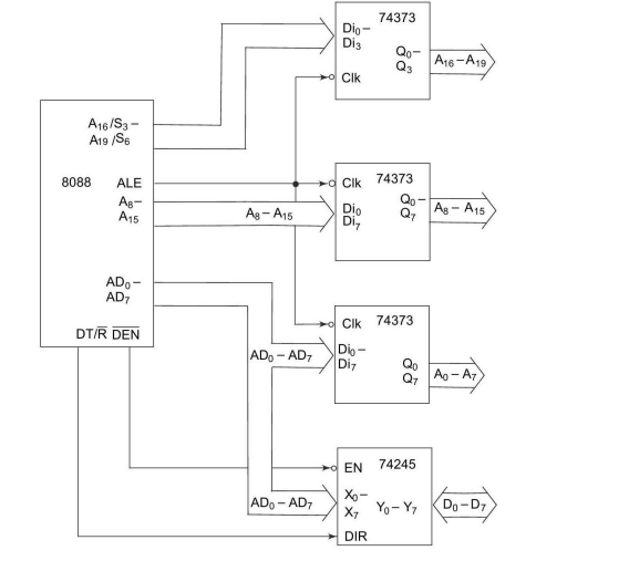
Deriving 8088 Bus
Deriving the 8088 bus involves understanding the architecture and signals used by the Intel 8088 microprocessor to communicate with external devices. Here’s a comprehensive guide from A to Z:
A. Address Bus (AD[19:0]):
- Description: The 8088 uses a 20-bit address bus to address up to 1 MB of memory.
- Function: It carries the memory address or I/O port address for read and write operations.
B. Bus Control Signals:
- Description: Various control signals manage bus operations such as read, write, and bus arbitration.
- Examples: RD (Read), WR (Write), M/IO (Memory/Input-Output), DT/R (Data Transmit/Receive), DEN (Data Enable), ALE (Address Latch Enable).
C. Clock Signal (CLK):
- Description: The clock signal synchronizes internal operations and external communication.
- Function: All processor activities are synchronized with the rising and falling edges of this signal.
D. Data Bus (D[7:0]):
- Description: The 8088 uses an 8-bit data bus for data transfer between the microprocessor and external devices.
- Function: Data is transmitted bidirectionally on the data bus during read and write cycles.
E. Error Handling Signals:
- Description: Signals indicate error conditions during bus operations or data transfers.
- Examples: ERROR (Bus Error), BHE (Bus High Enable), BE0/BE1 (Bus Error), etc.
F. Flow Control Signals:
- Description: Signals manage the flow of data and control signals between the processor and external devices.
- Examples: HOLD (Hold Request), HLDA (Hold Acknowledge), READY (Ready), LOCK (Bus Lock).
G. General-Purpose Registers:
- Description: Registers used for general data storage and manipulation within the microprocessor.
- Examples: AX, BX, CX, DX, SI, DI, BP, SP.
H. Handshaking Protocol:
- Description: Protocol ensures proper synchronization between the microprocessor and external devices during data transfer.
- Function: Signals such as DT/R, DEN, and READY facilitate data transfer and acknowledge completion.
I. Interrupt Signals and Control:
- Description: Interrupt signals allow external devices to interrupt normal execution flow.
- Examples: INTR (Interrupt Request), INTA (Interrupt Acknowledge), NMI (Non-Maskable Interrupt), etc.
J. Jump Instructions:
- Description: Instructions alter the program flow by jumping to different memory locations.
- Examples: JMP (Unconditional Jump), JZ/JNZ (Jump if Zero/Not Zero), JC/JNC (Jump if Carry/No Carry).
K. Keyboard/Display Interface:
- Description: Interface for connecting external devices such as keyboards and displays.
- Function: Enables communication between the microprocessor and input/output devices.
L. Logic Instructions:
- Description: Instructions perform logical operations such as AND, OR, XOR, and NOT.
- Function: Used for bitwise manipulation and logical comparisons in program execution.
M. Memory Management Unit (MMU):
- Description: The MMU manages memory access and translation between logical and physical addresses.
- Function: Translates logical addresses into physical addresses, enforces memory protection, and handles memory segmentation.
N. Numeric Coprocessor Interface:
- Description: Interface connects an optional numeric coprocessor (e.g., 8087) to the microprocessor.
- Function: Enhances mathematical processing capabilities by offloading floating-point arithmetic operations.
O. Opcode Fetch Unit:
- Description: Retrieves instructions from memory or external devices for execution.
- Function: Fetches instructions based on the address provided by the instruction pointer (IP) register.
P. Power Supply and Reset Signals:
- Description: Signals provide power and reset the microprocessor.
- Examples: VCC (Power Supply Voltage), GND (Ground), RESET (Reset Signal).
Q. Queue Management:
- Description: Manages instruction and data queues for efficient processing.
- Function: Prefetches and buffers instructions to optimize execution and reduce latency.
R. Read/Write Control Signals:
- Description: Signals control read and write operations on the system bus.
- Examples: RD (Read), WR (Write), DT/R (Data Transmit/Receive).
S. Stack Operations:
- Description: Operations manage the stack for subroutine calls and data storage.
- Examples: PUSH (Push Data onto Stack), POP (Pop Data from Stack), CALL (Call Subroutine), RET (Return from Subroutine).
T. Timing Diagrams:
- Description: Diagrams illustrate timing relationships between signals and operations.
- Purpose: Helps visualize and analyze signal timing and synchronization.
U. Unconditional Branches:
- Description: Instructions change the program flow unconditionally.
- Examples: JMP (Unconditional Jump), CALL (Call Subroutine), RET (Return from Subroutine).
V. Vector Processing:
- Description: Handles interrupt vectors and interrupt requests.
- Function: Points to interrupt service routines for handling external events.
W. Wait States:
- Description: Inserts wait states to synchronize with slower external devices or memory.
- Purpose: Ensures proper timing alignment and data integrity during bus transactions.
X. x86 Instruction Set:
- Description: The 8088 supports a comprehensive instruction set for data manipulation and control.
- Examples: Arithmetic, logical, data movement, control transfer, and string manipulation instructions.
Y. Yield Analysis:
- Description: Analyzes manufacturing yield and defect rates.
- Purpose: Ensures reliable production of microprocessors and informs process optimization efforts.
Z. Zero Flag (ZF) and Conditional Branching:
- Description: Indicates whether the result of an operation is zero.
- Usage: Conditional branching instructions depend on the state of the Zero flag.
Understanding the architecture and signals of the 8088 microprocessor is crucial for designing and interfacing with systems based on this iconic processor.
Comparison between 8086 and 8088
The comparison between the Intel 8086 and 8088 microprocessors involves understanding their similarities and differences across various aspects of architecture, performance, and application. Here’s a comprehensive guide from A to Z:
A. Address Bus Width:
- 8086: Features a 16-bit address bus.
- 8088: Utilizes a 20-bit address bus.
B. Bus Interface:
- 8086: Employs a 16-bit data bus.
- 8088: Uses an 8-bit data bus.
C. Clock Speed:
- 8086: Typically operates at a clock frequency of 5 MHz.
- 8088: Commonly runs at 4.77 MHz.
D. Data Bus Width:
- 8086: Utilizes a 16-bit data bus.
- 8088: Employs an 8-bit data bus.
E. Execution Unit:
- 8086: Features a 16-bit internal data bus.
- 8088: Incorporates an 8-bit internal data bus.
F. Functional Compatibility:
- 8086: Fully compatible with the 8088.
- 8088: Compatible with most software written for the 8086.
G. General-Purpose Registers:
- 8086: Includes AX, BX, CX, DX, SI, DI, BP, SP.
- 8088: Possesses the same set of general-purpose registers as the 8086.
H. Hardware Interrupts:
- 8086: Supports a wide range of hardware interrupts.
- 8088: Provides similar hardware interrupt capabilities as the 8086.
I. Instruction Set:
- 8086: Offers a rich instruction set with 16-bit operations.
- 8088: Shares the same instruction set architecture (ISA) as the 8086.
J. Jump Instructions:
- 8086: Supports unconditional and conditional jump instructions.
- 8088: Offers the same set of jump instructions as the 8086.
K. Keyboard/Display Interface:
- 8086: Provides interface capabilities for keyboards and displays.
- 8088: Incorporates similar interface functionalities as the 8086.
L. Logic Instructions:
- 8086: Includes logical operations such as AND, OR, XOR, NOT.
- 8088: Supports the same logical instructions as the 8086.
M. Memory Management:
- 8086: Features a 16-bit address bus for memory addressing.
- 8088: Utilizes a 20-bit address bus for memory addressing.
N. Numeric Coprocessor Support:
- 8086: Supports optional numeric coprocessor (e.g., 8087) for floating-point arithmetic.
- 8088: Compatible with the optional numeric coprocessor in the same manner as the 8086.
O. Opcode Fetch Unit:
- 8086: Retrieves instructions from memory or external devices for execution.
- 8088: Shares the same opcode fetch unit functionality as the 8086.
P. Power Supply and Reset Signals:
- 8086: Utilizes standard power supply and reset signals.
- 8088: Employs similar power supply and reset signal configurations as the 8086.
Q. Queue Management:
- 8086: Manages instruction and data queues for efficient processing.
- 8088: Incorporates queue management functionalities similar to the 8086.
R. Read/Write Control Signals:
- 8086: Controls read and write operations on the system bus.
- 8088: Employs similar read/write control signal mechanisms as the 8086.
S. Stack Operations:
- 8086: Supports stack operations for subroutine calls and data storage.
- 8088: Provides stack operation functionalities identical to the 8086.
T. Timing Diagrams:
- 8086: Follows timing diagrams for signal synchronization and operation timing.
- 8088: Adheres to timing diagrams similar to those of the 8086.
U. Unconditional Branches:
- 8086: Allows unconditional branching to alter program flow.
- 8088: Includes the same unconditional branching capabilities as the 8086.
V. Vector Processing:
- 8086: Handles interrupt vectors and requests for external event handling.
- 8088: Features vector processing functionalities comparable to the 8086.
W. Wait States:
- 8086: May insert wait states for synchronization with slower devices or memory.
- 8088: Employs wait states in a manner similar to the 8086.
X. x86 Instruction Set:
- 8086: Supports the x86 instruction set architecture.
- 8088: Utilizes the same x86 instruction set as the 8086.
Y. Yield Analysis:
- 8086: Subject to yield analysis for manufacturing efficiency and defect reduction.
- 8088: Undergoes yield analysis processes similar to those applied to the 8086.
Z. Zero Flag (ZF) and Conditional Branching:
- 8086: Utilizes the ZF flag for conditional branching based on zero/non-zero results.
- 8088: Incorporates the ZF flag in conditional branching operations in the same manner as the 8086.
By comparing the features and functionalities of the Intel 8086 and 8088 microprocessors, users can gain insights into their differences and similarities, enabling informed decisions in selecting the appropriate processor for specific applications.